Lapping Carrier by Photo-Etchinng
Importance of Surface Treatment
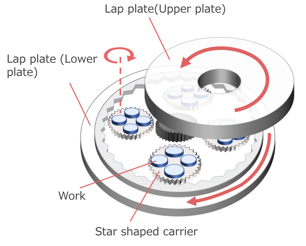
Ensuring silicon wafers are uniformly smooth is critical in semiconductor manufacturing. Silicon ingots, second only to diamonds in hardness, undergo challenging processing to achieve the atomically smooth surfaces required for semiconductor production. Lapping carriers are pivotal in the polishing process post-ingot cutting.
Lapping Process and Lapping Carrier
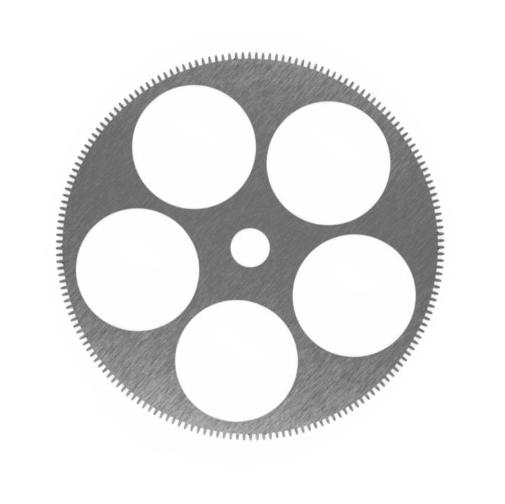
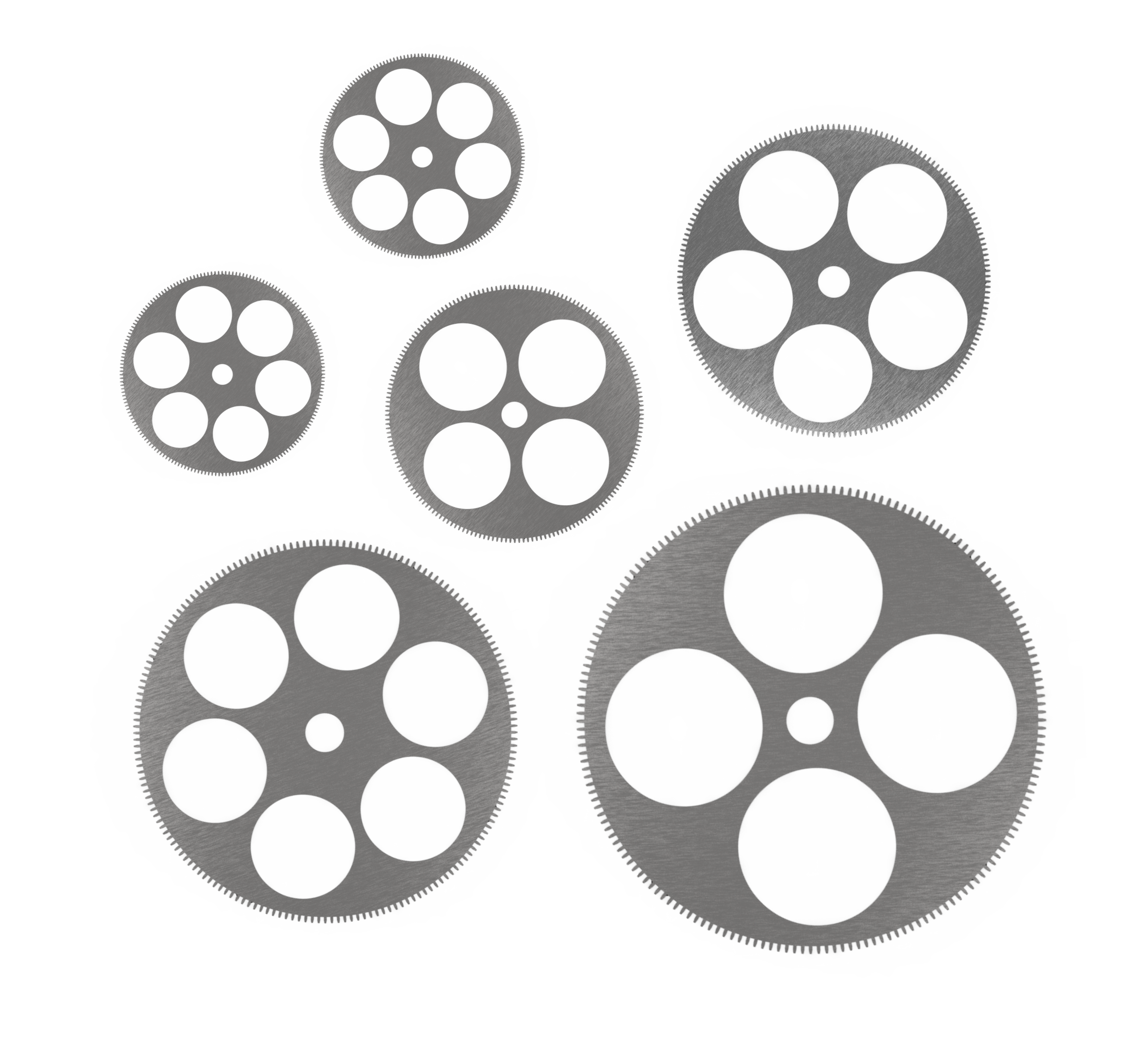
The silicon wafer is sliced from ingots, undergoes a lapping process to achieve smooth surfaces. The lapping carrier is featuring a central hole for wafer mounting and a gear for machine operation, securely holds the wafer between upper and lower plates. This setup ensures precise polishing of the wafer's surfaces, demanding high strength and flatness for effective support in narrow gaps.
Challenges of Lapping Carrier
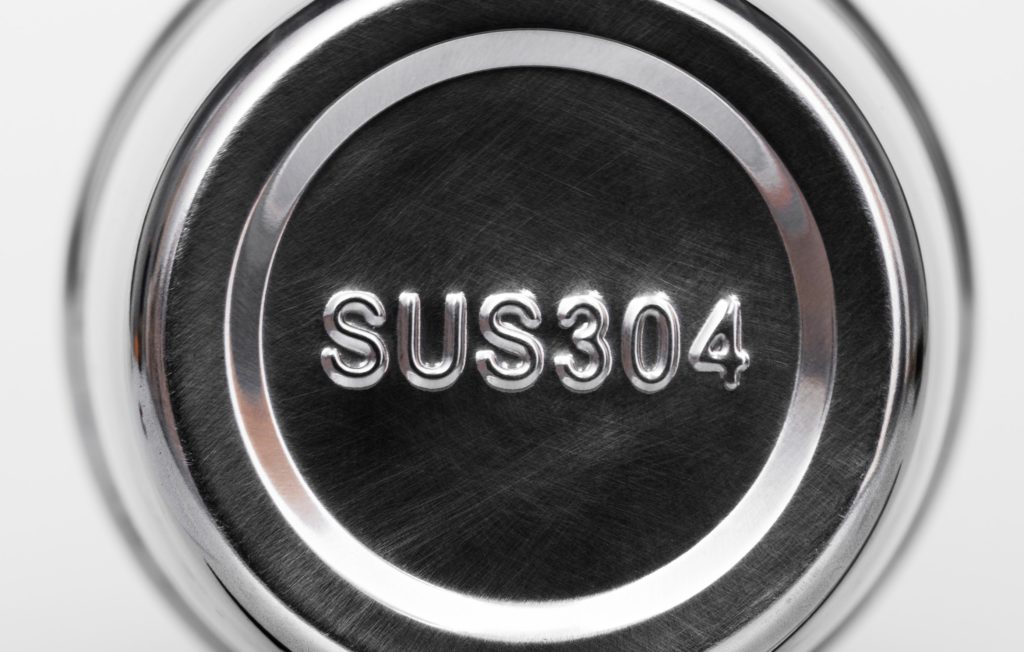
To enhance semiconductor manufacturing productivity, lapping machines are increasing in rotational speed and accommodating various thicknesses. Choosing the optimal lapping carrier requires a pre-review considering strength, warping, and measures against dimensional fluctuations from storage. SUS304 is a preferred material, although slight dimensional changes may occur over time, necessitating careful selection of processing methods based on required accuracy.
Proposal
We propose the lapping carrier manufactured by UPT using the photo-etching process.
Advantages
- Photo-etching process is good at small-quantity and quick delivery, which minimize the potential warp and deformation due to short inventory storage period.
- Initial investment for photo-etching technology is only for mask fee.
- Select the best material from UPT’s wide range stock. It enables to make ideal strength and less warp wrapping carrier.
■Example
Material: SUS304
Thickness: 0.2mm
Work size: φ100mm
Outer frame size: 300mm
■Capability
Material: All metals for etching process availability
Thickness: 0.004mm~
Machining accuracy: <10% of metal thickness
Process: Photo-etching
Value ①
High dimensional accuracy of ±10% of plate thickness with only 1 week delivery time
Our etched lapping carrier ensures minimal warp and deformation, using high-quality thin metal sheets without burrs or foreign material. With accuracy within 10% of material thickness, our solution offers easy lead-time management, enabling on-demand procurement and reducing storage time to prevent degradation.
Value ②
Supports large lapping Carrier Lapping Carriers
We are capable of processing up to 500mm x 500mm in size and can flexibly handle the production of lapping carrier of various sizes.
Value ③
Enough Inventory
We stock 500 varieties of materials and thicknesses, such as SUS304 in 5μm increments from a base of 50μm. This enables simultaneous testing of multiple lapping carriers for accuracy and strength confirmation.