Enhancing Semiconductor Production Efficiency through Precision Thermal Control
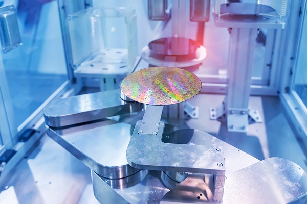
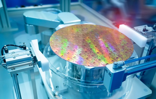
As semiconductor designs shrink, precise thermal control is vital in manufacturing. Particularly in the front-end process, heat management impacts throughput significantly. With the prevailing 300 mm wafer size, uniform heating of all chips is crucial for optimal yields. Temperature discrepancies within a wafer can lead to decreased yield rates. Semiconductor manufacturing involves multiple equipment stages, with wafers maneuvered by electrostatic chucks. These chucks utilize static electricity to securely hold wafers without damage, with modern versions featuring integrated heaters. This enables precise temperature regulation, compensating for variations in plasma density and cooling gas distribution across the wafer surface.
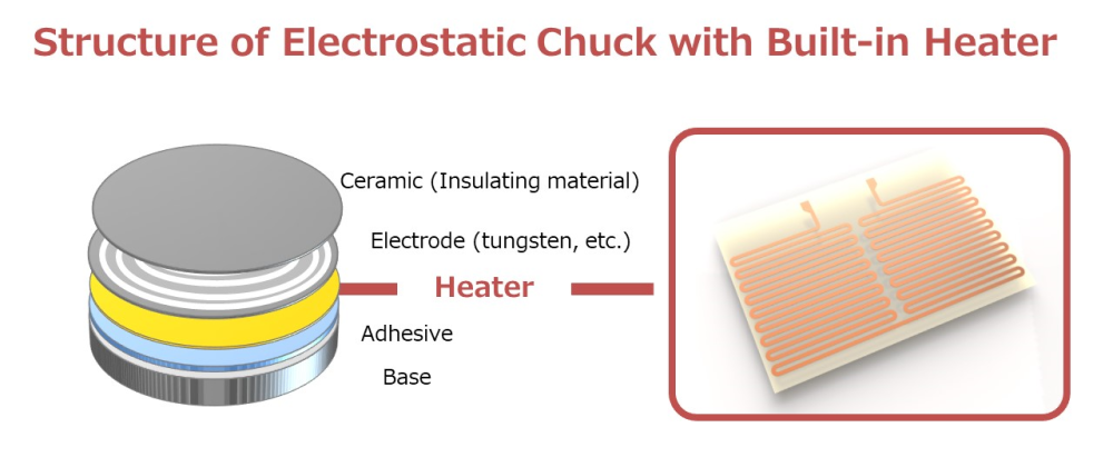
Electrostatic Chuck with Built-in Heater
What is the Electrostatic Chuck?
An electrostatic chuck is a device that holds objects in place using electrical force. The advantages of an electrostatic chuck include its ability to operate in vacuum environments and its capacity to hold objects, such as wafers, without causing damage. Therefore, electrostatic chucks are widely utilized in the manufacturing processes of ultra-precision equipment, such as semiconductor manufacturing.
Challenges of Electrostatic Chuck with Built-in Heaters
Effective heater design is crucial for evenly heating semiconductor wafers, especially large ones exceeding 300mm. The heating capacity of the metallic foil used in the heater increases, necessitating more complex designs for the foil's cross-sectional size and path to raise its resistance value for the required heat generation. Additionally, modifications are needed as heat performance depends not only on heater design but also on the ceramic plate on which the heater is mounted.
Proposal
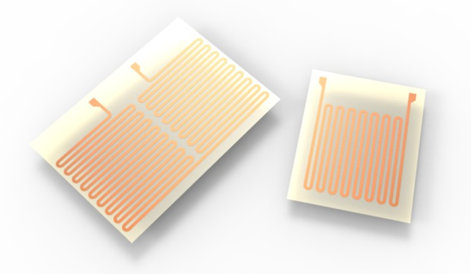
UPT offers etched metal foil heaters.
Advantages
- UPT deliver small quantities and wide variety of products, and supports timely if customer requests numerous minor design
- Support up to 450 mm wafers
- UPT preforms the etching process of the copper foil coated with polyimide (PI)
- UPT have a reliable quality system that inspects all the products to ship out to customers
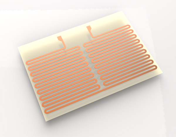
Product Overview of Heaters for Electrostatic Chucks
Maximum Processing Size: 500mm
MInimum Processing Width: 30μm
Metal Thickness More Than 50μm
Processing of copper foil only and etching of PI (polyimide) and other materials supplied with insulators
Value ①

Microfabrication Accuracy is ±20% of Plate Thickness
The etching process achieves an accuracy within ±20% of the plate thickness, with no burrs or particles present. Additionally, the etching process does not require expensive molds, resulting in very low costs, even with multiple trial and verification cuts.
Value ②

Supports Large Heaters
Given that UPT can process etching up to a size of 600mm x 900mm, we can also apply heaters for 450mm wafers. We possess extensive experience in the application of 300mm wafers with high productivity.
Value ③

Best in Class of Inspection System
The introduction of image inspection equipment equipped with AI technology has begun mainly at mass production plants. The system's ability to detect defective products continues to improve day by day. We are building a complete quality system by improving both inspection yield and quality.
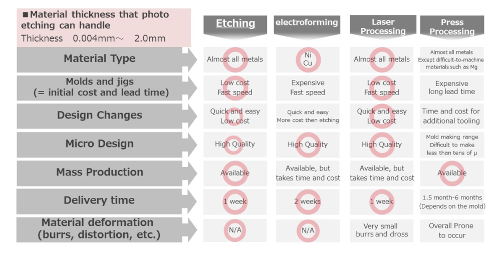
Specification List
- Target Metal Type: Copper
- Target Metal Thickness: 50μm~
- Machining Accuracy: Etching process accuracy: <20% (Relative to metal thickness) applicable for single-side etching
- Surface Treatment: Copper Sheets, either bare or insulated with materials like polymide, are provided for the etching process


