Test Socket for Miniaturized and Narrow-Pitch Semiconductor IC Test
IC test sockets are essential components that connect semiconductor devices to test equipment, enabling accurate evaluation of electrical performance and reliability. As device integration advances, sockets must support higher frequencies, greater current capacity, and finer terminal pitches.
UPT’s MMS (Micro Metal Socket®) is an innovative test socket developed through advanced metal processing and precision design. It offers ultra-low contact resistance, excellent high-frequency characteristics up to 60 GHz, and outstanding durability for next-generation semiconductor testing. Custom designs are available to meet diverse package shapes and test conditions.
For high-performance IC test sockets, trust UPT’s MMS — delivering precision, reliability, and flexibility for your semiconductor testing needs.
What is IC Test Socket?
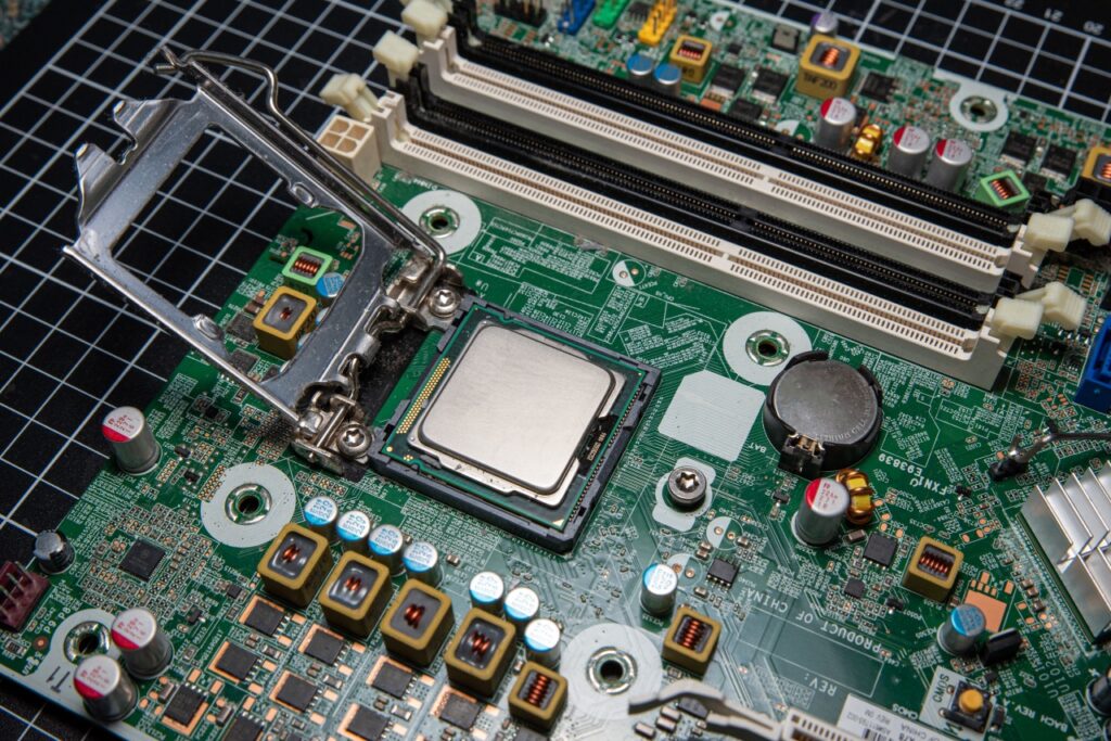
An IC test socket is an essential component used to evaluate the performance of advanced semiconductor devices, serving as the interface between the device and the test equipment.
It ensures stable electrical contact and precise mechanical alignment during testing, enabling accurate signal transmission and measurement. The quality and design of the IC test socket directly affect the accuracy and reliability of the evaluation results, especially in high-frequency and fine-pitch applications.
About MMS – An Innovative IC Test Socket
MMS is an innovative test socket designed to meet the demands of evolving semiconductor technology. As the need for high-frequency and high-current compatibility increases, semiconductor testing needs high performance. Additionally, sockets that can accommodate the miniaturization of semiconductors and narrower terminal pitches are required. MMS addresses these needs, contributing to the development and production of next-generation semiconductors.
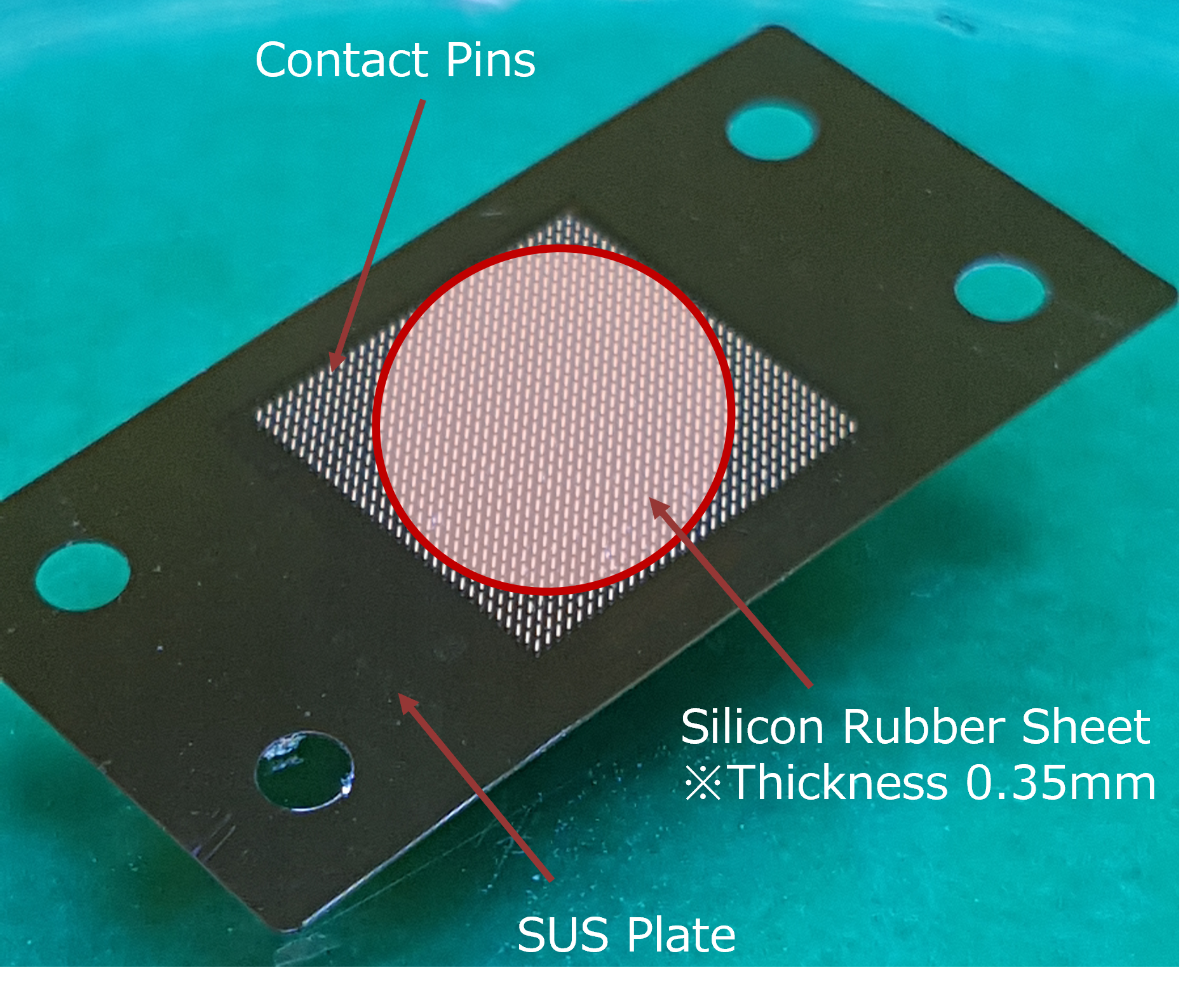
Micro Metal Socket®

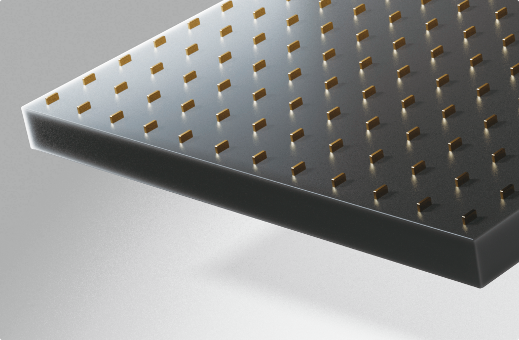
The holes for socket mounting can be freely arranged.
Key Feature
- Min contact height: 0.45mm
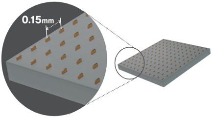
- Min contact pitch: 0.15mm
- High-frequency transmission characteristics with ultra-short transmission paths (60GHz @ -1dB)
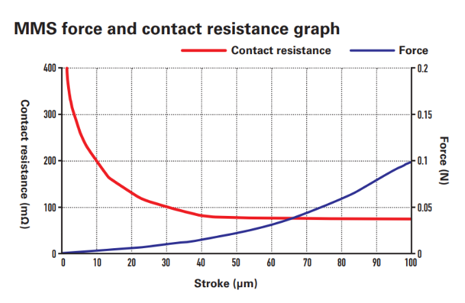
- Force / displacement: 0.10N / 0.1mm
Performance
- Supports high-speed/frequency transmission at 60GHz @ -1dB
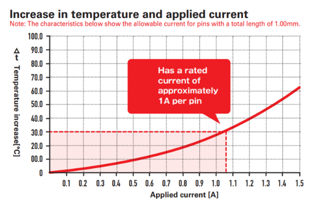
- Rated current: 1A per contact (with a contact height of 0.45mm)
Note: We offer the optimal product based on the dimensions, terminal pitch, and load requirements of the device under test.
Advantages of MMS
1.Unique Materials for High-Frequency and High-Current Applications
MMS achieves high-frequency transmission through ultra-short paths by developing micro contacts with a minimum contact height of 0.45mm. Even at 0.45mm contact height, MMS supports a rated current of 1A, eliminating the issues caused by contact resistance in semiconductor package tests and enabling more stable test processes.
2.Proprietary Contact Structure For Low Force Load and Reliable Contact
MMS uses a single-piece contact structure. Without internal contact structures, MMS achieves a low load of 0.10N per contact, reducing the stress on test handlers by approximately 80% compared with conventional sockets. Additionally, as a sheet-type contact for high-frequency measurement, MMS reaches both electrical and mechanical lifespans of 50,000 touchdowns.
3.Industry-Leading Minimum Contact Pitch
MMS supports miniaturization, multi-pin, and narrow-pitch applications, with a pitch as small as 0.15mm, ideal for next-generation semiconductor tests. The housing-free structure allows for customizable sheets tailored to specific applications and requirements, supporting both smartphone packages and future semiconductor technologies requiring narrow-pitch solutions.
Examples of MMS Applications
Narrow-Pitch IC Packages
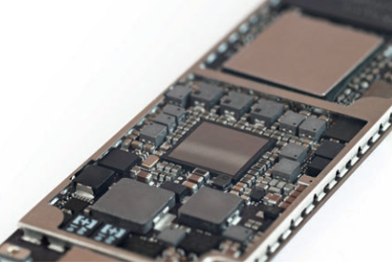
As semiconductor technology advances, IC packages become more compact, high-performance, and highly integrated, leading to narrower pitches. MMS, with a minimum pitch of 0.15mm, is the perfect solution for next-generation testing and even further advanced IC packages.
High-Pin-Count BGA Packages
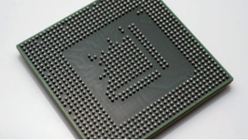
The pin counts of BGA packages are increasing, and more low force is required at the final test phase. MMS supports low force of 0.10N per pin (1/5 of conventional sockets), extending the lifespan of test equipment.
Interposer

MMS is also ideal for use as an interposer, offering pin layouts customized for specific IC package and board designs.
Camera Modules
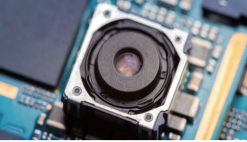
MMS is a suitable solution for the testing of high-resolution camera modules as well, because MMS supports stable connection with high-frequency.
Communication Modules
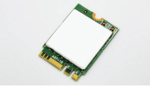
MMS provides stable high-frequency connectivity, making it a reliable choice for test communication modules.
Use Cases of MMS
Use Case 1: Semiconductor IC Final Test
Customer’s Challenge
It is difficult to measure high-frequency (millimeter-wave) signals stably using pogo-pins or rubber sockets.
UPT’s Solution
MMS is a one-piece structure and supports stable high-frequency characteristics. UPT solves this issue by customizing the design.
FAQ
-
Can MMS be customised to a specific device under test (DUT)?
-
Yes. MMS is provided in custom configurations according to DUT dimensions, terminal pitch, and load requirements. Mounting holes can also be arranged freely to match your board design.
-
Can MMS be integrated into existing test handlers or load boards?
-
Yes. MMS can be adapted to most existing test environments. Mounting holes, alignment features, and interposer interfaces can be customized to fit your equipment.
-
What is the lead time for design and delivery?
-
For standard configurations, typical lead time is about 6–8 weeks after specification confirmation. For fully customized sockets, it may extend depending on complexity.
-
Can UPT assist with socket + interposer co-design?
-
Yes. UPT offers design support for integrated test solutions that combine MMS with interposers or custom guides to optimize signal integrity and alignment.
-
Is evaluation or sample testing available before purchase?
-
Evaluation samples or trial sockets can be arranged for performance verification. Contact UPT for sample availability and testing support.
