Smallest, Thinnest, and Finest
UPT’s Photo Etching Technology Support the Hard-to-Process Materials, and Unique Shapes.
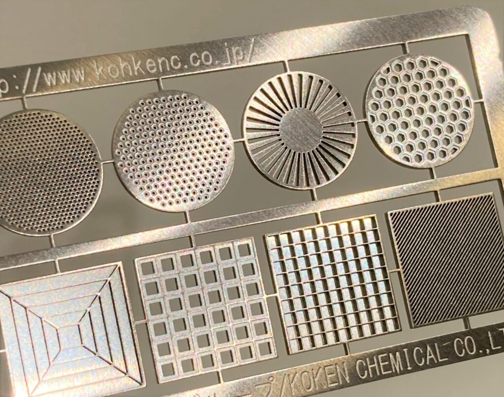
What’s Photo Etching Technology?
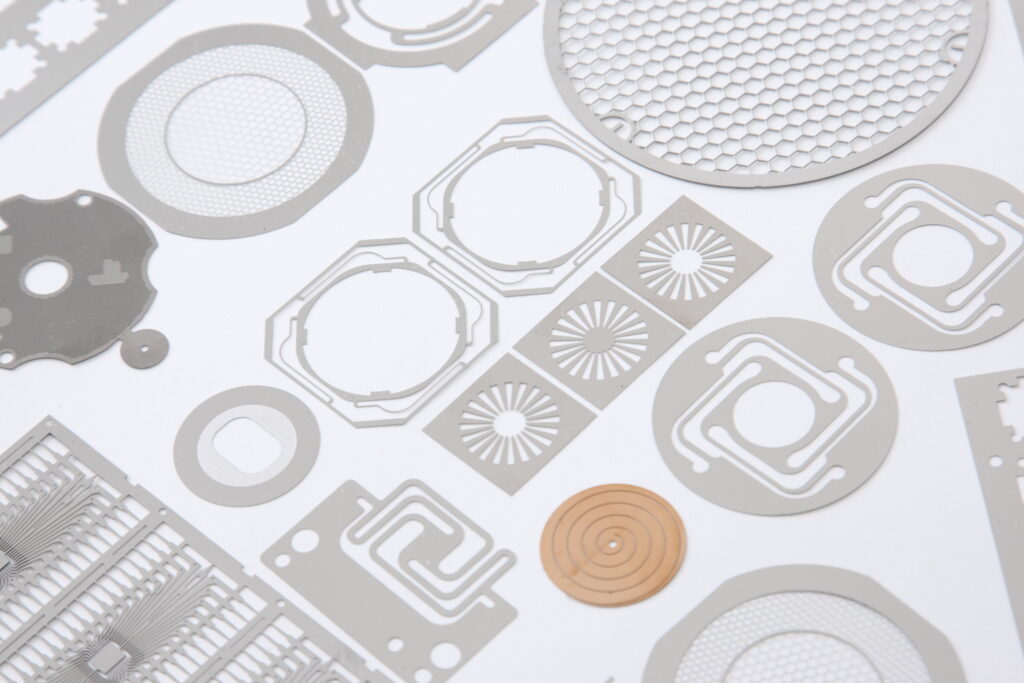
Photo etching technology is the process of using corrosive chemicals liquid to melt the specific areas on a metal sheet, and forms precise, unique and complex metal parts. This technology is able to form super fine shaping with high precision. Metal processed products need to be highly reliable because they need to maintain their performance over long periods of use and in harsh environments.
UPT offers “One-Stop Solution” of metal processed parts which support from prototype samples to mass production with short lead-time.
Benefits of Photo Etching Technology and Use-case
One of the major benefits of photo etching is that it processes metal without mechanical force, minimizing the risk of material deformation or damage. In addition, high precision processing is achieved by using photoresist to etch the specific area. Also, photo etching technology can be etched a wide range of materials, and it allows to maximize manufacturing flexibility and efficiency.
This technology is mainly used in the manufacturing equipment for electric components and semiconductors, such as jigs and small components which require extremely fine patterns and complex designs.
What UPT’s Photo Etching Technology?
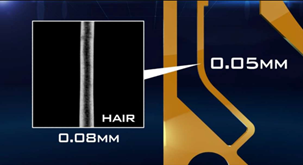
Smallest, Thinnest, and Finest
UPT has proven track record of achieving top market share for high precision metal components used in smartphones. Our technology enables the processing of hard-to-process materials, and various thickness materials whose range is from 0.004mm to 2mm. UPT can support and help as your partner across all applications with technological innovation together.
We constantly research new technologies to improve product performance and to reduce costs for customer satisfaction and market adaptation.
High Quality, Low Cost, and Short Lead-Times
We have implemented the equipment and quality control systems we have developed in Japan factories to overseas factory located in Thailand, enabling to achieve low-cost mass production with high quality. We have a wide range of materials, over 500 types in stock always, and the dedicated prototyping team, in order to support quick response and short lead-time.
UPT’s Reliable Response (One-Stop Solution)
UPT supports various processing requirements of customers in one stop, from design to manufacturing, plating and machining etc. By coordinating and managing external 3rd party suppliers. This allows our customers to improve their production efficiency. In addition, we have the mass production factories in Japan and Thailand, and support multiple languages, not only Japanese but also English, Chinese, Korean and Thai.

Processable Materials
Stainless
SUS301、SUS304、SUS430、SUS316、SUS631
Nikkel silver
Ni201、36Ni、42Ni、Permalloy
Steel
SPCC
Titanium
TR270C
Aluminum
A1050、A1100、A5052、A6061、A6063
Copper/ Copper alloy
C1020、C1100、C1720、C2680、C2801、C5191、C5210、C7521、C7701
Kovar
KV-2、KV-6
Carbon steel
SK5
Applications of Photo Etching Technology
Semiconductor Test Solutions
Photo etching technology enables the processing of metals with excellent conductivity and durability with high dimensional accuracy. This strength is suitable for manufacturing probe pins and test sockets, which are key components in semiconductor test equipment. UPT offers the “Union Contact®” (one-piece probe pin) and “Micro Metal Socket®” (test socket).
Thermal Solutions
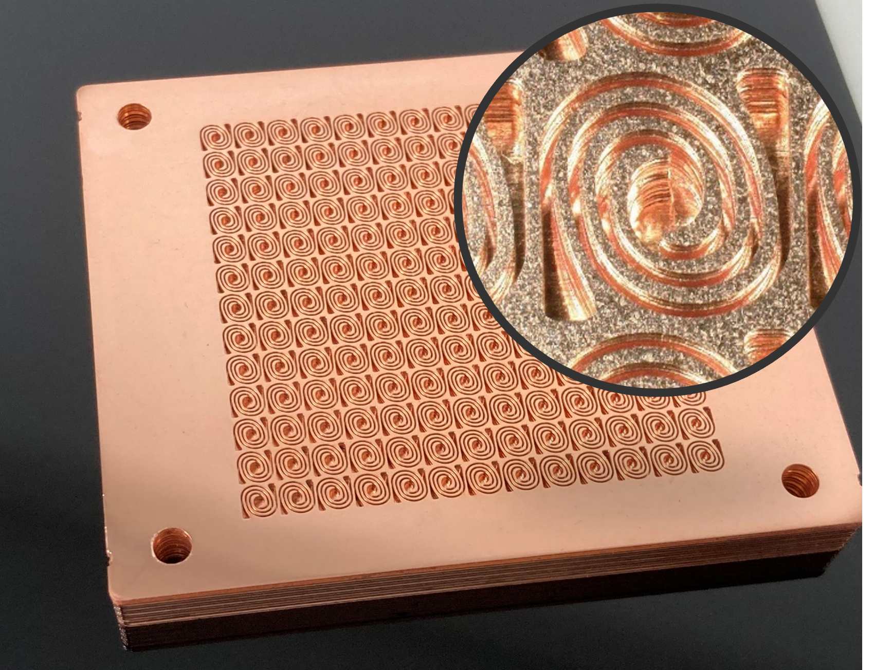
Photo etching technology has an excellent capability to form very fine flow paths used in thermal solutions such as cold/cooling plate and heat sink. This technology is suitable for applications which require high cooling performance to process complex patterns with high precision in metal sheets which have a high thermal conductivity. We offer thermal solutions for various types of cold/cooling plates and heat sinks.
Shims
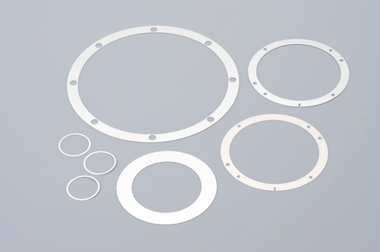
Photo etching technology can process metal foils/plates and sheets with high precision, and it's an ideal solution for manufacturing gap adjustment components like shim spacers. This technology allows for consistent production of exact thickness and shape even with ultra-thin materials, making it valuable for applications requiring high accuracy.
High-Precision Filters
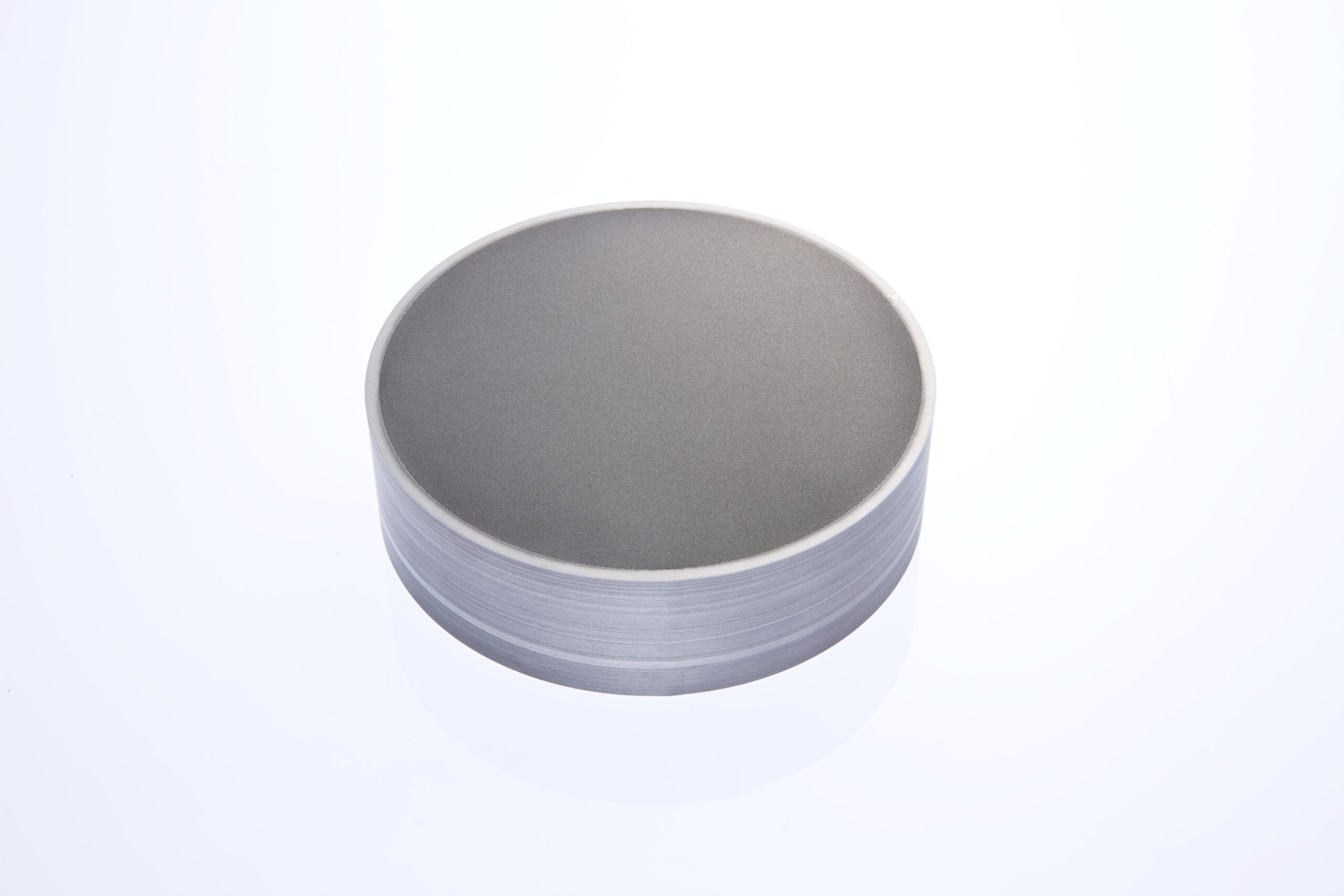
Photo etching is suitable for manufacturing high-precision filters that can remove fine impurities from liquids and gases or perform precise flow control. It has ability to precisely process fine holes and complex patterns.
Photo Etching Technology with Diffusion Bonding Technology
We have created new value such as following items by combining photo etching and diffusion bonding technology.
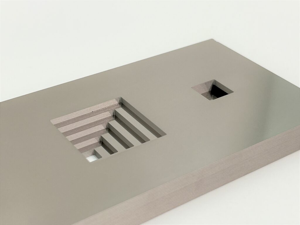
Thickness 0.5mm×10
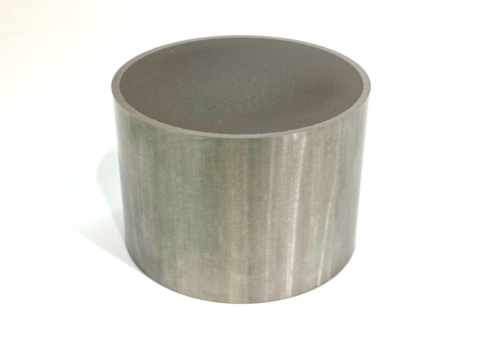
Thickness 0.05mm×1,000
Thickness 0.1mm×7
Benefits of Photo Etching + Diffusion Bonding Technology
- Capable of handling complex and intricate designs
- High Reliability in harsh environments (such as high and low temperature)
- High fracture toughness and high temperature resistance
- Little post-bond alignment error
- High dimensional accuracy
- Little deformation
- Available to form 3D shapes and flow paths impossible with machining
- Cost-effective from prototyping to mass production