
The demand for process automation in the electronic component industry is motivated by several factors. These include the need to enhance the efficiency and productivity of industrial processes, ensure better quality control, and meet the increasing demands of global supply chains. As specialists of precision metal fabrications, we've leveraged our wealth of experience to engineer fabrication jigs and other solutions aimed at optimizing industrial processes.
Jig Trays by Diffusion Bonding
Our Precision Jig Trays for micro-size electronic components are crafted using cutting-edge photo etching and diffusion bonding technologies, redefining precision, efficiency, and quality control . Tailored to your unique component specifications, our Union Tray® Jig Trays deliver unmatched precision, eliminating errors, and optimizing production.
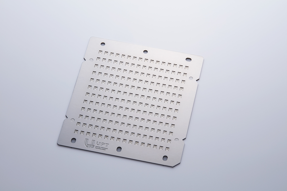
- Unmatched Precision &Customization
Photo etching allows for intricate and precise designs, ensuring that each processing jig tray can be tailored to meet the exact specifications and requirements of your components. - Cost-Effective
The absence of expensive molds or tooling reduces initial setup costs, making it a cost-effective solution for both prototyping and mass production. - Durability
The combination of materials and bonding techniques ensures that the processing jig trays have a long lifespan and can endure harsh manufacturing environments. - Short Lead Times
Photo etching and diffusion bonding processes are relatively quick, allowing for shorter lead times in production, which is crucial for time-sensitive projects.
Talk to Us about Your Project
Since our Processing Jig is fully customizable to fit your device/equipment, please don't hesitate to reach out to us with your ideas.
Process Mask by Diffusion Bonding
Our deposition masks, made through photo etching and diffusion bonding, are used to create circuits, including those for ceramic capacitors and crystal oscillators. We offer a range of mask options, from single-layer film circuits to multi-layer film circuits produced using our proprietary method, which enables simultaneous bonding.
These masks ensure precision and durability, allowing us to create intricate designs with tight tolerances. They are robust and versatile, meeting the demands of various applications while accommodating specific requirements.
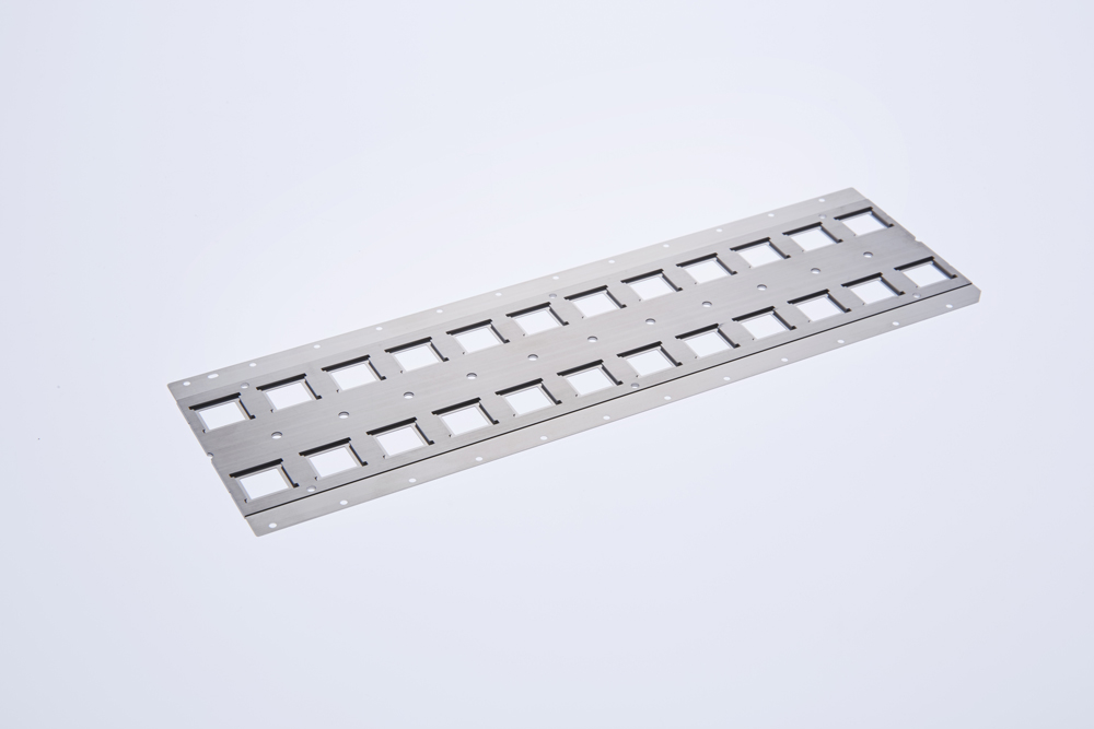
Features
- High Precision
Photo etching and diffusion bonding ensure the creation of masks with extremely fine details and tight tolerances. - Durability
These processes result in robust masks that can withstand the demands of high-volume production.
- Complex Geometries
Photo etching and diffusion bonding enable the production of masks with intricate and complex geometries that might be challenging to achieve through traditional methods. - Consistency
The combination of photo etching and diffusion bonding ensures consistent mask quality, crucial for uniform production.
Talk to Us about Your Project
Since our Processing Jig is fully customizable to fit your device/equipment, please don't hesitate to reach out to us with your ideas.