From smartphones to automotive electronic control units, metal masks are indispensable for printed circuit board (PCB) assembly. Did you know that the manufacturing method of the mask can significantly affect both mounting quality and cost?
In this article, we compare three major manufacturing methods—laser processing, etching processing, and electroforming—with particular focus on the advantages and applications of etching-based production.
What Is a Metal Mask?
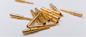
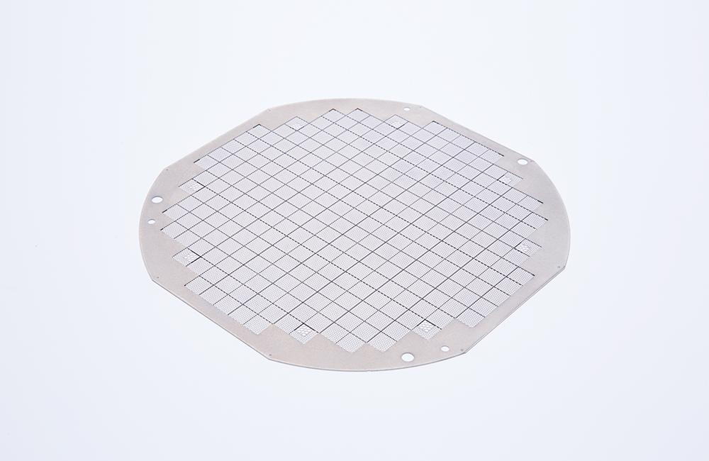
A metal mask is a thin metal stencil used for solder paste printing, the first step in the surface mount technology process.
Solder paste transfers onto the PCB through fine apertures aligned with pad positions, helping suppress defects such as bridging, voids, and insufficient solder after reflow.
Material
SUS304 and SUS430 are commonly used. Nickel alloys and Invar are also used.
Thickness
Typically 0.08–0.20 mm.
For example:
- 0.10 mm for boards mainly using 0402 chips
- 0.18 mm for boards with mixed through-hole technology (THT) components
Aperture Processing
Three methods are widely used in practice:
- Laser processing
- Etching
- Electroforming
Metal Mask Manufacturing Methods
| Item | Laser Processing (Mainstream) | Etching Processing | Electroforming |
| Typical Thickness | 0.08–0.20 mm | 0.10–0.30 mm(step thickness possible) | 0.02–0.15 mm |
| Aperture Accuracy (±) | 8–12 µm | 15–25 µm | 3–6 µm |
| Hole Wall Shape | Nearly vertical | Double-sided taper | Extremely vertical |
| Paste Release | ◎ Excellent | △ Improved with surface treatment | ◎ Mirror-like finish |
| Step Thickness | Achieved with additional plating, etc. | Achieved in a single process via half-etching | Local thickening possible via electroforming |
| Cost | Medium | Low | High |
| Lead Time | 2–4 days | 1–3 days | 5–7 days |
| Main Applications | High-density mass production | Thick plates, THT mixed boards, mid-volume production | 0201/01005 components, OLED fine metal mask |
| Advantages | Balance of fine precision and mass productivity | Strong for thick plates, large panels, and step structures | Ultra-fine precision with mirror walls |
| Disadvantages | Cost increases with the number of apertures | Not suitable for ultra-fine pitch | Expensive with longer lead times |
Note: Minimum pitch and other specifications vary depending on equipment. Please treat these values as general guidelines.
Advantages of Manufacturing Metal Masks With Etching
Zero Thermal Impact on the Base Material
Since etching dissolves metal through chemical reactions, it does not generate localized heat like laser processing.
This minimizes warping and distortion, allowing high flatness even for large panels or thick plates over 0.15 mm.
Step Structures Formed in a Single Process
By simply changing the resist pattern, half-etching creates step structures.
This allows a single mask to optimize the solder paste volume for boards that combine 0402 chips and large connectors.
Excellent Cost Performance for Mid-Volume Production
The same jig can process multiple apertures simultaneously, so unit cost decreases as production volume increases.
This makes the method suitable for production runs ranging from several hundred to several thousand units.
Short Lead Times
Since the process can be completed with standard photolithography equipment, a next-day turnaround is possible.
Major Types of Metal Masks Manufactured by Etching
Thick Masks for THT / Pin-in-Paste
Masks with a step thickness of 0.18 mm or greater enable dual-in-line connectors and chip components to be reflowed in a single pass.
High Thermal Capacity Masks for LED and Power Boards
These masks supply large volumes of solder paste to wide pads while suppressing mask warpage.
Vapor Deposition Masks
These masks are used for OLED and semiconductor thin-film deposition.
Etching combined with diffusion bonding ensures high-precision multi-stage cavities (see case study below).
Stencils for Adhesive or Coating Printing
These stencils reduce the risk of clogging, even with high-viscosity materials.
Hybrid Step Masks
These multi-layer stencils allow 0402 component areas and large connector areas to be handled with a single mask.
Metal Mask Manufacturing Case Study
UPT’s proprietary etching and diffusion bonding technologies were combined to address a challenge in vacuum deposition masks: creating multi-stage cavities measuring several tens of micrometers, along with numerous microholes, with high precision at low cost.
Structures that would suffer from distortion with laser processing, and high cost / long lead times with machining, were instead produced through batch etching and diffusion bonding, enabling precise step structures.
In addition, a magnetic fixing structure reduced assembly work, while dimensional variations caused by thermal expansion during deposition were also resolved.
Leave Your Metal Mask Manufacturing to UPT
UPT delivers advanced microfabrication solutions for semiconductor and electronic device industries under the motto:
“Smaller, thinner, and finer than anywhere else.”
Through photoetching and diffusion bonding technologies, UPT meets the most demanding requirements in advanced manufacturing.
High Quality × Low Cost × Short Lead Time
Global production bases and abundant material inventory optimize quality, cost, and delivery.
Integrated Production System
UPT handles everything in one place—from specification design to prototyping, mass production, and post-processing.
Multilingual Support
Support is available in Japanese, English, Chinese, and more for global projects.
If you have any questions regarding metal mask design or manufacturing, please feel free to contact us using the form below.