About probe pin
Probe pins contact the object under test and transmit electrical signals during electrical testing. It is critical to understand their characteristics and proper use for the reliable inspection process,.
Here’s the main features of probe pins:
Electrical conductivity
Highly conductive materials such as gold and beryllium copper are used to ensure accurate signal transmission. These materials enable probe pins to reliably detect even the smallest electrical signals and realize highly accurate inspections.
Contact stability
The spring structure maintains a constant contact pressure, guarantees uniform contact with the object to be measured, and improves measurement reproducibility. It also ensures stable contact even when the object surface condition changes.
High durability
Probe pins are designed to withstand repeated use, and measures against wear and fatigue are especially imprortant to maintain performance over extended periods.
Usage example
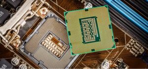
- Semiconductor wafer testing: inspection of the electrical characteristics of each die on the wafer
- IC package final test: functional verification of products after assembly
- Printed circuit board continuity test: confirmation of wiring pattern continuity
- Characterization of electronic components: inspection of components such as resistors and capacitors
- Inspection of automotive electrical components: confirmation of sensors and ECUs operation
In these inspection processes, as probe pin performance directly affects inspection accuracy and productivity, proper selection and control are essential.
Technical Challenges and Solutions
Dealing with poor contact
Contact failure is an important problem that directly affects inspection reliability. The main causes include oxide film on the surface of the object to be inspected, adhesion of foreign matter, and insufficient contact pressure. This problem is especially serious in the inspection of fine terminals and products operating at high speeds.
The following approaches are effective solutions:
– Proper contact pressure
Setting the optimum contact pressure in accordance with the object characteristics ensures stable contact. Excessive pressure may damage the object, while insufficient pressure causes poor contact.
– Optimization of tip shape
Surface treatment such as serration process destroys the oxide film and ensures reliable electrical contact. It is important to select the most appropriate processing method for each object’s material and surface condition.
– Establish periodic cleaning procedures
Appropriate cleaning intervals and methods should be established to prevent the accumulation of foreign matter and oxides. Adoption of effective cleaning methods, such as ultrasonic cleaning and use of specialized cleaners, is recommended.
– Surface treatment of contact area
Surface treatment such as gold plating improves oxidation resistance and conductivity. Plating material and thickness are determined in consideration of the operating environment and required durability.
Reduce wear and extend probe pin life
Though wear itself from repeated use is unavoidable, appropriate countermeasures can extend pin life. Especially in high-speed inspection and high-volume production lines, probe pin life has a direct impact on productivity.
The following factors should be considered:
– Appropriate material selection
The optimum material must be selected based on usage conditions such as temperature and contact frequency. For example, a material with high heat resistance is selected for high-temperature environments, while a material with excellent wear resistance is selected for high-frequency use.
– Rules for periodic inspections and replacements
Wear conditions should be quantitatively evaluated, and pins be replaced at the appropriate time span. Evaluation items include visual inspection, continuity testing, and contact resistance measurement.
– Adequate contact pressure
As excessive contact pressure accelerates wear, it is important to adjust the pressure to the minimum necessary to obtain stable contact. For pressure control, periodic checks using a dedicated measuring instrument are recommended.
– Adopt abrasion-resistant surface treatment
Surface treatments such as hard chrome plating and nitriding can improve wear resistance and extend pins’ life.
Improve measurement accuracy
To achieve accurate measurements, the following factors must be comprehensively considered:
– Stabilization of contact resistance
Contact resistance variations are minimized by securing the contact area and optimizing the surface treatment. Particularly in the measurement of minute signals, variations in contact resistance have a significant impact on measurement results.
– Noise reduction
Shielded construction and optimized wiring paths reduce the influence of external noise. In addition, high-sensitivity measurements require careful attention to grounding methods and cable placement.
– Temperature changes
Temperature control of the measurement environment and the introduction of a temperature compensation function can suppress measurement errors caused by temperature changes. In particular, the effect of temperature drift should be taken into account in continuous measurement over a long period of time.
– Accurate mechanical positioning
Stable contact is achieved by mounting the probe pins and their alignment with the object accurately.
Challenges in high-frequency and high-current measurements
High-frequency measurements have signal attenuation and crosstalk issues, and high-current measurements have heat generation and voltage drop issues. The followings can be effective solutions.
– Impedance matching
To suppresses signal reflection and attenuation, it is critical for module design to take into account the characteristic impedance of the transmission line . Careful attention should also be paid to the structure and placement of probe pins to maintain high-frequency characteristics.
– Shielded structure adoption
Proper shield design minimizes crosstalk and noise effects. It is also important to consider shield grounding methods and shielding between adjacent pins.
– Heat dissipation design
Adopting an effective heat dissipation structure to ease heat generation during high current measurement is crucial. Also, introducing cooling mechanisms using materials with high thermal conductivity should be considered.
– Appropriate cross-sectional area
Heat generation and voltage drop are suppressed by designing the conductor cross-sectional area in consideration of current density. However, it must be compatible with mechanical strength.
Points for probe pin selection
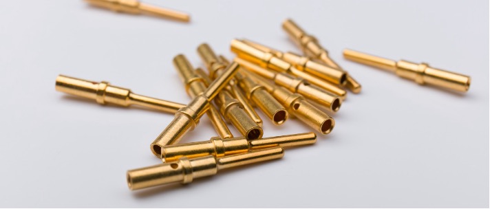
Pin type
– Spring
- Suitable for general applications with excellent cost performance
- Large stroke and high tolerance for misalignment
- Easy maintenance and parts replacement
- Various spring characteristics can be selected
– Cantilever
- Capable of handling minute pitches
- Lateral approach is possible
- Easy adjustment of contact pressure
- Scrubbing effect Improves contact stability
– Vertical
- Suitable for high-frequency measurements
- Easy impedance matching
- Miniaturization is possible
- High mechanical stability
Optimization of tip shape
– Conical shape
- Suitable for standard applications
- Stable contact point
- Suitable for a wide variety of objects
- Relatively low production cost
– Crown type
- Effective in removing oxide film
- Multi-point contact improves stability
- High scrubbing effect
- Require careful handling to avoid damage to the object
– Flat type
- Reduce pad damage
- Large contact area and low contact resistance
- Suitable for high current measurement
- Low tolerance for misalignment
– Needle type
- Capable of handling fine terminals
- Suitable for high-density mounting
- Easy to concentrate contact pressure
- Require attention to tip wear
Points for Material Selection
– Phosphor bronze
- Suitable for standard applications
- Good cost performance
- Well-balanced mechanical properties
- Excellent workability
– Beryllium copper
- Ideal when high strength and high conductivity are required
- Excellent fatigue resistance
- Suitable for high-temperature environment
- Relatively high price
– Tungsten
- Excellent abrasion resistance
- High hardness
- Low coefficient of thermal expansion
- Limited workability
– Precious Metal Alloys
- Used when high reliability is required
- Excellent corrosion resistance
- Low contact resistance
- High cost
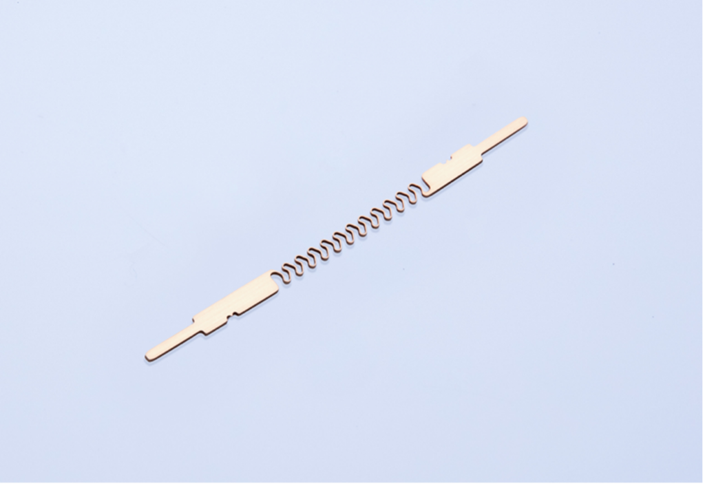
「Union Contact™」One-piece contact pin structure for high conductivity, low load, and long life.
「Union Contact™」probe pins for semiconductor inspection have an automatic one-piece structure that provides higher electrical conductivity and lower load. The long life of the probe pins also contributes greatly to cost reductions for our customers.
These features enable efficient and reliable semiconductor inspection. We can design taylor made「Union Contact™」in accordance with your requests. Please feel free to contact us for more information.