「どこよりも小さく・薄く・細く」
難削材、ユニークな形状など、さまざまな加工に対応
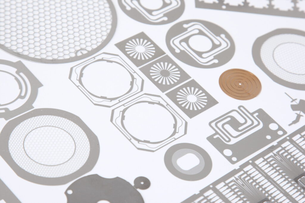
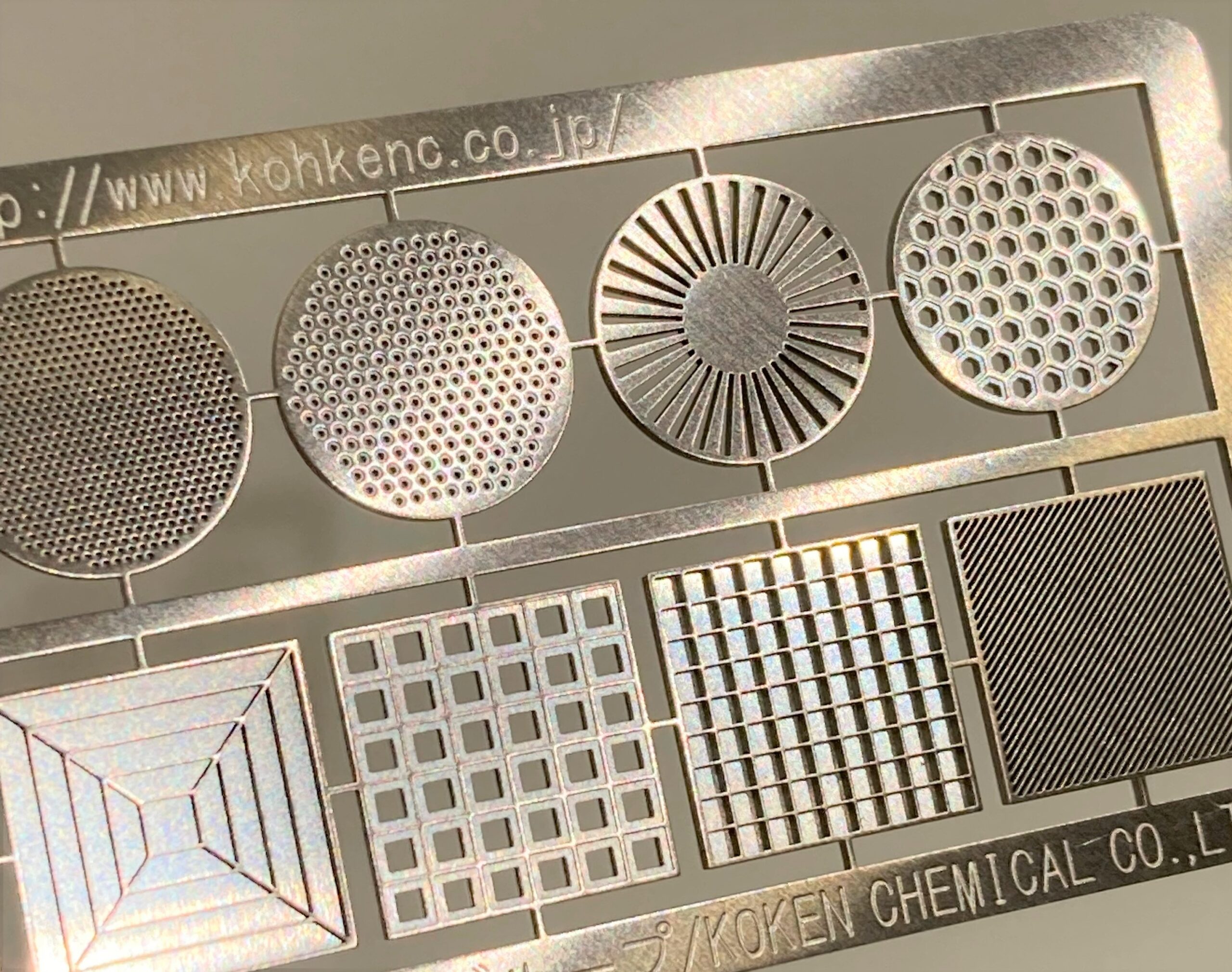
フォトエッチング技術は、薬液を使用して特定の部分のみ金属表面を腐食溶解させることにより、極細かつ複雑な金属部品を形成する加工方法です。フォトエッチング技術は微細な成形を可能とし、精度の高い加工が可能です。金属加工製品は、⾧期間の使用や過酷な環境下でも性能を維持する必要があるため、高い信頼性が必要とされています。
UPTでは、フォトエッチング技術を活用した金属加工部品の製造を、試作から量産までワンストップで対応しています。短納期の製造にも対応しておりますので、お気軽にお問い合わせください。
フォトエッチング技術の利点と使用例
この技術の大きな利点の一つは、物理的な力を加えずに金属を加工できるため、材料の変形や損傷のリスクを最小限に抑えられることです。また、フォトレジスト(感光性材料)を使用して特定の部分だけを保護し、残りの部分をエッチングすることで、高精度な加工を実現します。さらに、フォトエッチング技術は幅広い材料に対応可能なため、製造の柔軟性と効率性を高めることができます。
この方法は、特に半導体や電子機器製造の分野に欠かせない部品・治具の製造において重宝されています。極小の部品や極薄の板厚を持つ製品、さらには特殊で複雑な形状の部品製品の加工にも対応可能で、精密性が求められる場面で活用されています。
UPTのフォトエッチング加工技術の特徴
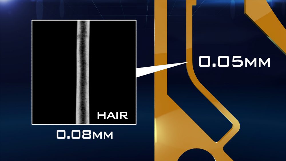
どこよりも小さく・薄く・細く
UPTは小型・薄型化が求められるスマートフォンの精密部品においてトップシェアを誇る開発・製造販売の実績があります。難削材と呼ばれる材料や最薄0.004mm~最大2mmの厚みのある材料まで、様々な形状の加工に対応し、あらゆるアプリケーションにおける技術革新のパートナーとしてお役に立ちます。
高品質×低コスト×短納期の追求
UPTでは、お客様のご要望や市場の変化に対応するため、製品の性能向上やコスト削減を目指す新技術を日々研究しています。
また、国内工場で培った設備・品質管理体制を海外工場(タイ)にも導入し、国産品質での低コスト量産を実現しました。
さらに、500種類を超える豊富な材料在庫と試作専門チームによる迅速な対応で、短納期を実現しています。
安心の対応力(ワンストップ・ソリューション)
UPTでは、仕様設計から製作、メッキや機械加工などの追加工程が必要な場合でも、外部の技術サプライヤーとの調整と管理を行い、ワンストップにてお客様の様々な加工要求に応えることができます。様々な生産ニーズに合わせたワンストップ・ソリューションを提供することにより、お客様の生産効率を向上させることが出来ます。
また、国内外に対応可能な一貫した量産体制を持ち、日本語、英語、中国語、韓国語、タイ語など、複数言語での対応が可能です。

対応可能な材質
ステンレス
SUS301、SUS304、SUS430、SUS316、SUS631
ニッケル/ニッケル合金
Ni201、36Ni、42Ni、パーマロイ
鉄
SPCC
チタン
TR270C
マグネシウム
マグネシウム合金
アルミ
A1050、A1100、A5052、A6061、A6063
銅/銅合金
C1020、C1100、C1720、C2680、C2801、C5191、C5210、C7521、C7701
コバール
KV-2、KV-6
炭素鋼
SK5
フォトエッチングの用途例
半導体テストソリューション

フォトエッチング技術により、導電性や耐久性に優れた金属を高い寸法精度で加工することができます。そのため、半導体テスト機器のキーパーツであるプローブピンやテストソケットの製造に適しています。 UPTでは、ワンピース構造のプローブピン「Union Contact®」や、テストソケット「MMS」などを製造販売しています。
サーマルソリューション
フォトエッチング技術は、非常に緻密な流路を正確に形成する能力に優れており、コールドプレートなどの微細流路が必要な部材の製造に適しています。この技術は、高い熱伝導性を有する薄板金属に複雑なパターンを高精度で加工できるため、冷却性能が重要なアプリケーションに役立ちます。UPTでは、コールドプレートやヒートシンクといったサーマルソリューションを製造販売しています。
シム関連製品
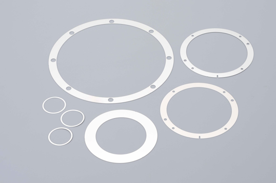
フォトエッチング技術は、非常に高い精度で金属箔/板を加工することが可能で、シムスペーサーのような隙間調整部材の製造に最適です。この方法では、極薄の材料でも正確な厚さと形状を一貫して製造できるため、高精度が要求されるアプリケーションに役立ちます。
高精度フィルタ
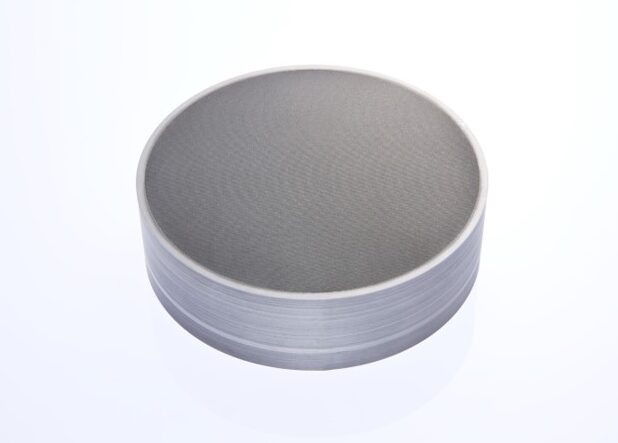
フォトエッチング技術は、非常に細かい穴や複雑なパターンを精密に加工できるため、液体や気体の細かい不純物の除去や、微細な流量コントロールを行うことができる、高精度フィルタの製造に適しています。
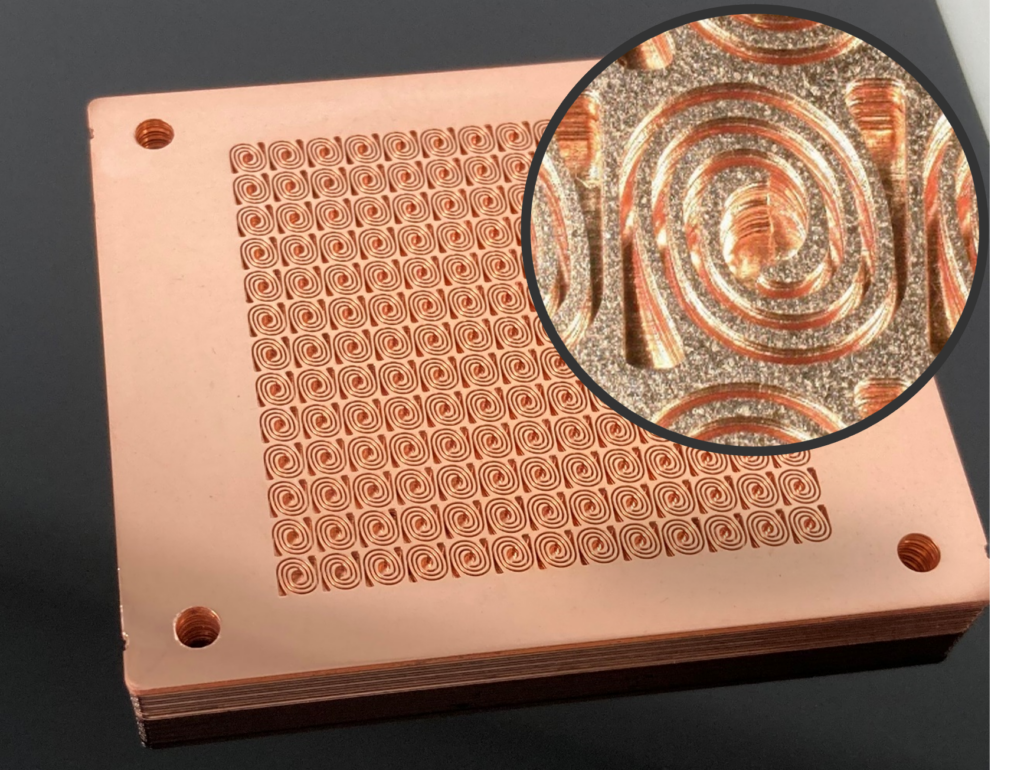
フォトエッチング+拡散接合により新たな価値を創造
UPTでは、フォトエッチングと拡散接合の技術を組み合わせることで新たな価値を創造してきました。技術の組み合わせにより生まれる特徴や製造加工イメージについてご紹介します。
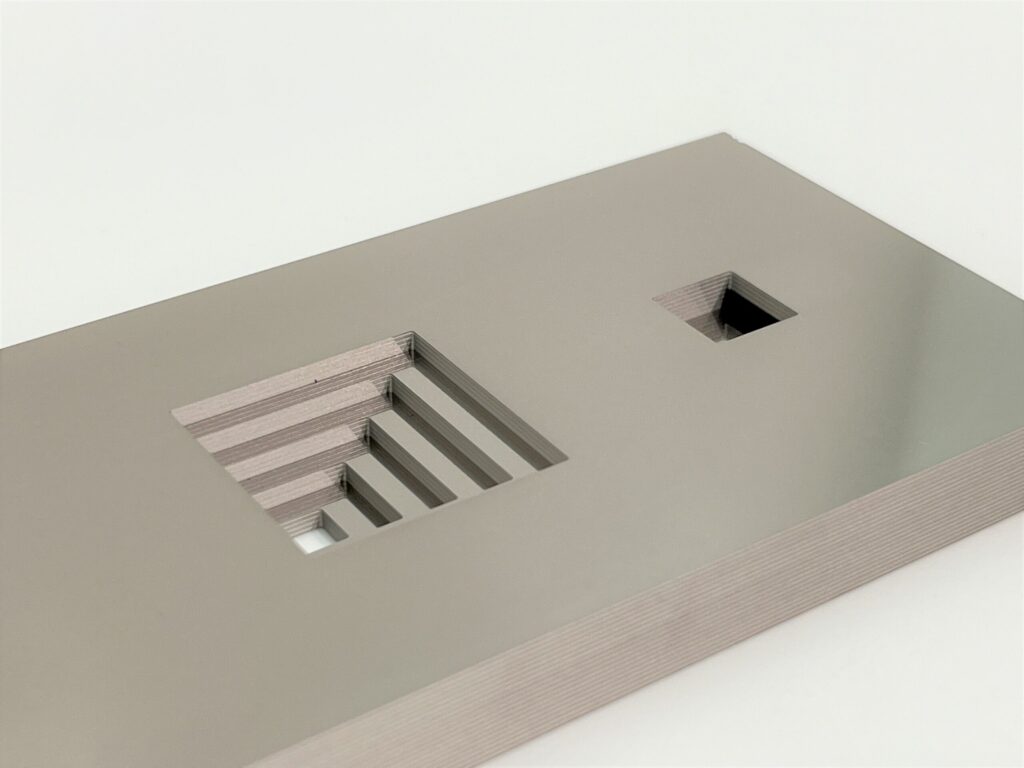
機械加工では不可能な立体構造
板厚0.5mm×10枚
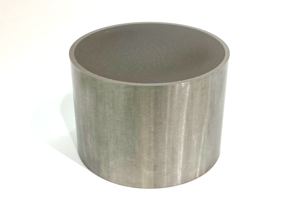
微細メッシュを拡散接合で重ねた高アスペクト比の金属フィルタ
板厚0.05mm×1000枚
複雑・微細デザインに対応
板厚0.1mm×7枚
フォトエッチング+拡散接合の特徴
- 複雑・微細デザインに対応可能
- 過酷な環境下(高温・低温)での使用において信頼性が高い
- 破壊耐性と耐熱性が高い
- 接合強度が高い
- 接合後のアライメント誤差が少ない
- 高い寸法精度
- 接合後の変形が少ない
- 機械加工では不可能な3次元形状や流路形成が可能
- 試作から量産までの費用対効果が高い