Metal LID Sealing for Electronic Components and Semiconductor Packages
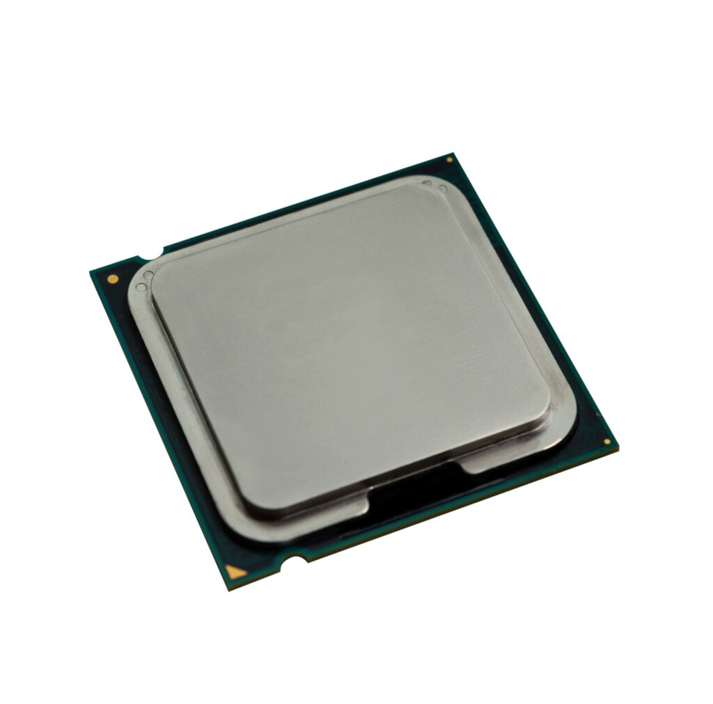
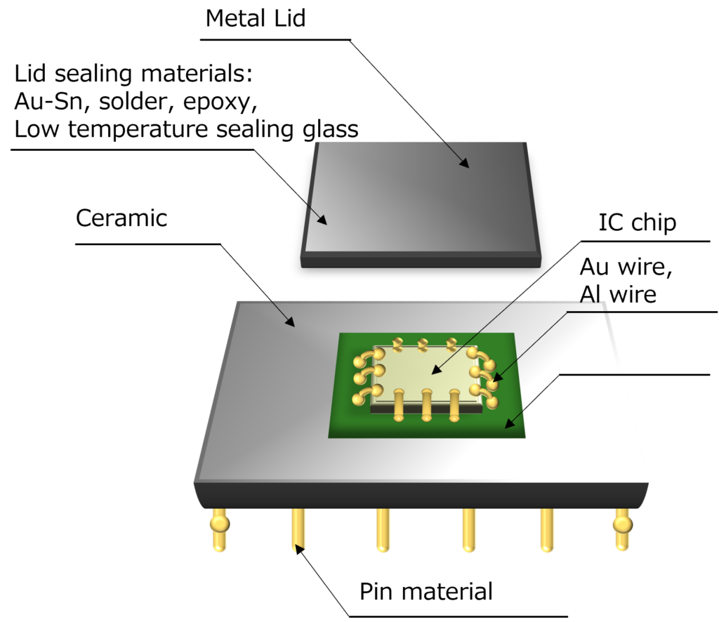
Semiconductor package is very important to secure the quality, and semiconductor package technology is becoming very important. The main roles for package are the heat dissipation and protection against external shocks. After the chip is mounted, it is sealed to protect the die inside the chip, and one method is to use a metal LID.
Use-Case of Metal LID
The quartz crystals, oscillators and SAWs are often used in smartphones and other devices, which is required durability against shocks. For this reason, some packages are made with ceramic and sealed with a metal lid.
Challenges of Metal LID
Bonding of metal LIDs to different materials such as ceramics is usually done with gold-tin solder or silver brazing. The challenge of sealing is to maintain bonding strength while inhibiting the flow the small particle into the package. There are many techniques to have better quality, however the cost may be higher due to the special process is required to meet the quality/reliability.
PROPOSAL
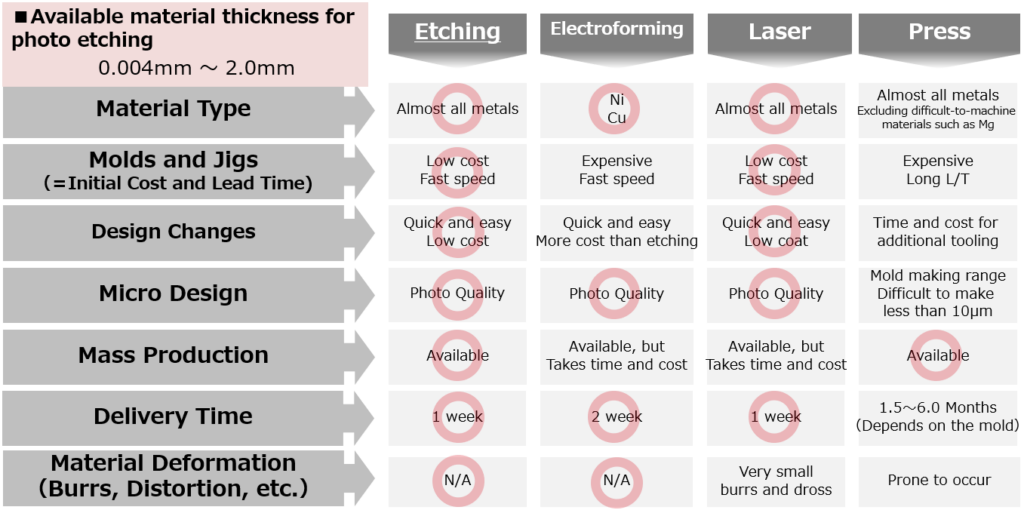
We propose photo-etched metal LID manufactured by UPT Group.
Advantages
- Allows processing of complex shapes required to improve sealing strength. Short delivery times allow for a cut-and-try process.
- The initial cost is only the mask fee, so customer can try different types of products to get the best dimensions.
- UPT Group always has a wide variety of materials in stock and can produce ideal LIDs in short lead time.
LID Products by Photo-Etching Process
Material: All metals that can be photo-etched ( Expect tungsten-based, gold and silver)
Thickness: Available in any thickness ( 0.04mm~)
Accuracy: Etching process accuracy: <10% ( Relative to metal plate thickness)
Processing Methods: Photo-Etching
Surface finishing: Gold plating and more
Value ①
High Quality Metal LID for Complex Shapes
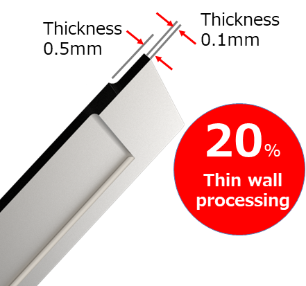
High-quality metal lids made through etching minimize warp and deformation with tightly controlled thin sheets, free from burrs and foreign material. Half-etching from both sides allows for complex and thin-walled shapes, up to 20% of material thickness. Photo etching also offers a quick lead time.
Value ②
Low Initial Cost: Just the Mask Fee for Easy Prototype Production Trials
Photo-etching is a technology that utilizes metal melting for processing products. The sole initial cost incurred is the mask fee. It’s a highly convenient method as it enables simultaneous evaluation of multiple products with varying LID materials and dimensions during the development phase. Final specifications can be determined after confirming compatibility with the package.
Value ③
Your Material Solutions Await
At our disposal are over 500 distinct materials and thicknesses readily available in stock. For instance, you can order five variations of SUS304 material, ranging from 50µm to 70µm in 5µm increments. This comprehensive selection enables simultaneous evaluation of machining accuracy and strength across multiple LID types. Additionally, even the challenging Kovar material is available for selection.